 Back to the Blog Index
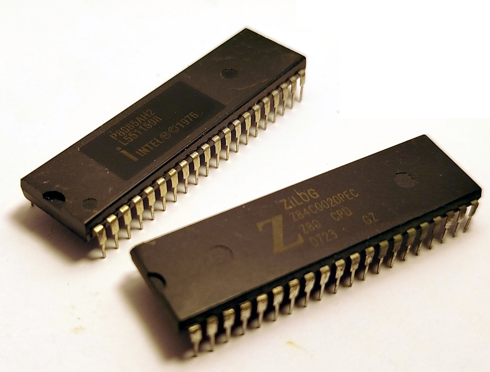
As of writing, the Zilog Z80 processor was officially launched 50 years ago, in July of 1976, less than 4 years after the last human had walked on the moon, decades closer to WWII than to the present day, roughly at a half way point between the Kennedy assassination and the fall of the Berlin wall, closer to the Korean war than to 9/11 which is itself an event that happened a quarter of a century ago. (Sorry…)
The processor was extremely successful, being used in many 8 bit microcomputers, including early personal computers, home & hobby computers, as well as many embedded, industrial applications.
Together with the 8080 & 8085 that it is binary compatible with, it contributed to creating a de facto hardware standard for 8 bit micros, allowing a de facto software standard of CP/M, and Microsoft BASIC.
The Z80 itself also spawned many clones and derived architectures over the years, famously including the Sharp LR35902, used in the original GameBoy. Zilog themselves eventually gave up their line of 16 and 32 bit derived architectures and returned to Z80 based microcontrollers and variants like the pipelined and higher clocked eZ80, mainly for continued use in industrial applications.
I myself am much too young to have seen the home computing side of this (ignoring the aforementioned GameBoy), but the widespread use in industrial applications means that the original Z80 is still around and in use with Zilog finally discontinuing it mere 2 years ago.
My own first encounter with the Z80 was as a late teenager, when I was browsing an electronics company catalog, surprised to find them still being sold. I designed my own little Z80 computer and convinced a school teacher to let me use the photo lab at night, so I could etch some PCBs.
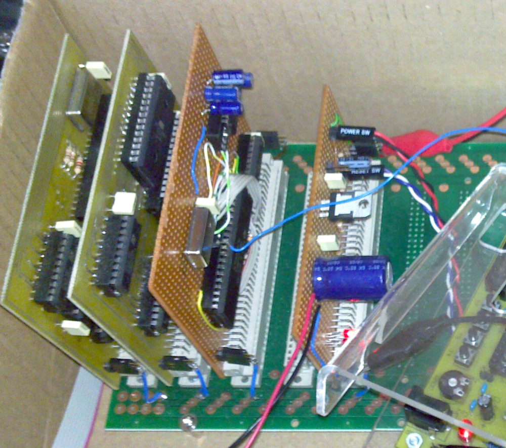
As several of my former teachers got curious what I was up to, I ended up hearing a lot of interesting anecdotes about old home computers, consoles and a story about DIY wire wrap computer in a Tupperware box, running CP/M and WordStar, hooked up to a "borrowed" IBM terminal that was used to write a thesis on. Over time I ended up being gifted a number of old chips from dusty drawers that made it into my own DIY project, including a bunch of MCS-85 parts, several Z80s, 8085s, 6502s and 6522s.
The whole thing sure taught me a number of interesting lessons about systems engineering and some unexpected ones (reliable power-on reset is surprisingly hard; writing a linker is a lot harder than writing an assembler, writing a compiler is something you can actually do).
Anyway, that is my claim to being allowed to reminisce about the Z80. While I originally wanted to limit myself to some technical details based on my own experience, comparing the Z80 with the 8080 that it was derived from, I ended up diving down a rabbit hole of the Computer History Museums oral history panel, where the people involved recalled even more anecdotes about the development of those chips. The whole "I'll try to write a blog post (again)" idea quickly ballooned in scope.
Once upon a time, the Computer Terminal Corporation (CTC) built a new, programmable terminal, the Datapoint 2200, sporting an 8 bit processor constructed from individual TTL chips. Intel was supplying CTC with shift registers and memory chips at the time.
The idea was floated to replace parts of TTL cemetery with custom ICs, eventually it was considered to try and get the entire 8 bit CPU on a single chip. Two different companies were ultimately contracted for this task: Texas Instruments and Intel.
Neither company finished their design in time. When Intel had the chip ready, originally named 1201 based on a systematic naming convention, CTC were already selling terminals based on the TTL design.
Engineers at CTC were also unsatisfied with the performance of the chips and they had already made changes to the architecture for the next generation of the terminal anyway.
While TI ultimately canned their design, Intel went ahead and successfully commercialized their version as the 8008 (like the 4004, renamed by marketing).
        ___   ___
-9V ---|1  |_| 18|<- IRQ
AD7 <->|2      17|<- READY
AD6 <->|3      16|<- CLK1
AD5 <->|4      15|<- CLK2
AD4 <->|5      14|-> SYNC __
AD3 <->|6      13|-> S0     |
AD2 <->|7      12|-> S1      > State
AD1 <->|8      11|-> S2   __|
AD0 <->|9      10|-- +5V
       |_________|
|
|
||||||||||||||||||||||||||||||||||||||||||||||||||||||||||||||||
The 8008 has 7 registers: A, B, C, D, E, H, L. Where A is the designated accumulator, the others can be used as operands or scratch. As the name might imply, H and L together form the High and Low part of a memory pointer. Accessing memory is done through an 8th pseudo register M, representing the memory byte that HL points to.
The processor internally keeps track of ALU state (Cary, Parity, Zero, Sign) in a few flag bits on which it can perform conditional jumps (including call and return).
The program counter PC is pretty much never visible directly. There are dedicated function call & return instructions, but the processor uses an internal return address stack that is 8 levels deep. The reason for this was that the Datapoint 2200 was originally supposed to use serial memory, a call stack in memory was considered to end up a performance bottle neck.
Memory addresses are 14 bits wide, there is a separate I/O address space with a total of 32 I/O ports (the addresses are always immediate and bit-stuffed into the opcode).
For interrupt handling, there is a special "restart" instruction that essentially calls into 1 of 8 slots (0x00, 0x08, 0x10, 0x18, ..., 0x38) at the beginning of the address space. The slot index is bit-stuffed into the RST opcode itself. When an interrupt occurs, the processor signals to the periphery that it got the hint and then blindly executes the current contents of the data bus that better be an RST instruction.
From there, it gets a bit tricky. The CPU does not have a general purpose stack that it can safe registers to, all memory access needs HL, but you don't want to clobber HL in the interrupt handler. The intended way to solve this was through external latches on the I/O bus, serving as scratch registers.
All in all, the architecture is fairly simplistic, requiring about 3500 transistors and used a DIP18 package. Address and data were multiplexed, requiring external latching. Internal decode/execution state was exposed that needed to be decoded to drive latches and figure out what the processor is attempting to do (read from or write to memory, or the I/O bus).
The processor needed two phase-shifted clock signals (it ran at 500kHz), a +5V positive supply and -9V negative supply.
The shortcomings of the Datapoint 2200 derived 8008 architecture were known during development, and in typical engineering fashion, before development was even wrapped up, ideas were thrown around for an improved architecture.
Federico Faggin, who was brought over from the 4004 project, was pushing to start work on an improved version, but management insisted to first see how the market would react to their two microprocessors. Competitors eventually announced their own 8 bit designs in the making and the delays ended up costing Intel a total of 9 months of their lead time.
Even before the project was finally approved, Federico Faggin got approval to hire Masatoshi Shima away from Busicom to work on the 8080 design. In many ways similar to how CTC had a hand in the development of the 8008, Busicom was involved in the development of the 4004, originally wanting a set of custom chips for their calculators.
Criticism and feedback from potential customers that the 8008 was demonstrated to, also influenced the design of the 8080, and it was decided early on to set aside binary compatibility.
| A | F |
| B | C |
| D | E |
| H | L |
| SP | |
| PC | |
The 8080 has in essence the same register set as the 8008, but it replaces the internal return address stack with an external one that lives in memory and is accessed via a stack pointer register (SP).
The stack pointer can be exchanged or moved in to/out of HL, registers can be pushed on or popped of the stack pairwise. Besides HL, the other register pairs are BC, DE, and AF (accumulator and ALU flags), but the 8080 assembly prefers to call the later the "program status word" PSW.
Memory addresses are bumped up to full 16 bits, giving the machine a 64k address space. The I/O ports are bumped up to 256. BC and DE now also allow rudimentary indirection (loading/storing the accumulator), the accumulator and HL can be loaded/stored at an immediate destination.
A few double-byte arithmetic operations are added that can work on register pairs (e.g. increment/decrement), mainly to allow pointer arithmetic and 16 bit counters. Using those instructions on AF would actually act on SP instead.
Interrupt handling works much the same way, using restart instructions, but with the added feature that interrupts can be enabled/disabled in software. An explicit stack also no longer requires saving registers using I/O hardware.
Here is a slightly modified memory-copy example from the Wikipedia page, it copies a number of bytes (stored in BC) from DE to HL.
memcpy:
    PUSH    B           ; pushes BC
    PUSH    D           ; pushes DE
    PUSH    H           ; pushes HL

loop:
    LDAX    D           ; A := *(DE)
    MOV     M, A        ; *(HL) := A
    INX     D           ; ++DE
    INX     H           ; ++HL
    DCX     B           ; --BC

    MOV     A, B        ; A := B
    ORA     C           ; A |= C
    JNZ     loop        ; jump if not zero

    POP     H
    POP     D
    POP     B
    RET
A few things that are noteworthy here: instructions that act on register pairs always use a single register as a mnemonic for both, the "X" ion the "INX" differentiates the double-byte increment from an "INC" on a single register byte. The 8080 assembly has an almost 1:1 mapping of mnemonics to opcodes and is extremely easy to parse, making an assembler easy to implement. To a degree, this comes at the expense of human readability.
Furthermore, the double-byte arithmetic has no influence on the ALU flags, it is a separate, independent function block. After decrementing BC, we need to manually check if both registers are zero.
To improve speed, the 8080 used NMOS logic. The downside of this was the the CPU now needed 3 different supply voltages (-5V, +5V and +12V). It also stuck with using 2 phase-shifted clock signals (in the 9V to 12V range), making electrical design around the chip a bit cumbersome.
Thanks to a 40 pin package (something Faggin recalls as an uphill battle to get approved), the CPU no longer had to multiplex data and address lines. But like the 8008, it still exposed internal processor state externally, multiplexing the actual control states on the data bus, requiring external latching and decoding.
Intel would of course sell support chips for state decoding, clock generation and so on. Additionally, one might also want to buy an accompanying interrupt controller and something like a programmable interval timer, at the very least to drive DRAM refresh, possibly using one of those handy Intel DMA controllers.
Intel addressed at least some of those short comings with the 8085, only requiring a single 5V supply and a single 5V clock signal. The freed up pins expose a few additional control signals. But still needing some specialized support chips.
Dissatisfied with his experience at Intel, the delays and uphill battles with management to even get the 8080 project approved in the first place, Federico Faggin finally decided to quit Intel and start his own firm together with Ralph Ungermann, then head of the microprocessor division.
Originally somewhat directionless, Faggin at first considered designing a microcontroller, but realized that the margins were too tight to make it economical for a fabless semiconductor startup.
He eventually settled on designing an improved version of the 8080, nicknamed "Super 80", later becoming the Zilog Z80. They secured funding from Exxon and also brought over Masatoshi Shima from Intel to work on the design, later increasing the size of the team to a total of 11 people to work on layouting, software simulation, and so on.
The design of the Z80 was intended to be binary compatible with the 8080, while adding registers, addressing modes, new instructions, drawing inspiration from other contemporaries like the 6800. It also aimed at simpler electrical interfacing and higher speed than the 8080.
The entire development of the processor up to the first, working prototypes cost roughly $400k, finishing on time and under budget (they had secured $500k from Exxon).
Zilog relied on Mostek to manufacture their processors (after some hostilities with Synertek they initially contracted with). They did eventually secure further funding from Exxon to build their own fab, but kept second sourcing the Z80.
| A | F | A' | F' |
| B | C | B' | C' |
| D | E | D' | E' |
| H | L | H' | L' |
| IX | |||
| IY | |||
| SP | |||
| PC | |||
The Z80 is fully binary compatible with the 8080 instruction set.
Inspired by the 6800, it adds two index registers IX and IY that can be used in place of HL (same encoding but with an opcode prefix) and with an immediate offset.
The AF, BC, DE and HL register pairs are bank switched, allowing simpler & faster interrupt handling.
Speaking of interrupts, the Z80 has 3 different ways that it can handle them: An 8080 compatible way (mode 0), one that always calls to a fixed location (mode 1), and one that dispatches through a call table (mode 2), using the number on the bus as an index. An extra register is used to locate the base of the table in memory.
The Z80 also adds a bunch of bit rotate, bit test & set instruction instructions, BCD arithmetic, along with built-in loop instructions (using BC as a counter), self-repeating block transfer, block compare and string operations.
Because Intel claimed a copyright on the assembly mnemonics, the Z80 ended up using its own assembly language with an arguably cleaner syntax. The Z80 assembly expresses operands more explicitly and uses overloaded variants of basic mnemonics.
This is essentially the same program from above, in the more expressive Z80 assembly:
memcpy:
    PUSH    BC             ; full name of the register pair
    PUSH    DE
    PUSH    HL

loop:
    LD      A, (DE)        ; explicit 2 argument syntax
    LD      (HL), A
    INC     DE
    INC     HL
    DEC     BC

    LD      A, B            ; overloaded name
    OR      C
    JP      NZ, loop        ; overloaded name, condition is an argument

    POP     HL
    POP     DE
    POP     BC
    RET
Of course, on the Z80, the entire byte copy loop could also be replaced with a single, self-repeating instruction: LDIR.
The Z80 only needs a single 5V supply and a single clock signal. Many of the externally latched/decoded states of the 8080 are explicitly exposed by the chip, such as as MREQ or IORQ to indicate memory or I/O access, RD/WR signals that indicate exactly what the name suggests, and an M1 signal that indicates the current memory access is an instruction fetch. Those signals can be connected to something as simple as a single 74xx138 to drive an (E)EPROM, some form of RAM and an UART controller. Connect the address and data lines directly to the Z80 and you essentially have a working computer!
If the RAM in use happens to be DRAM, the Z80 can also take care of DRAM refreshes, using an internal refresh counter that it puts on the address bus during instruction decoding cycles, asserting a control line to tell the external decoding logic to do a DRAM refresh.
With interrupt mode 1, where the CPU always calls to a hard wired location, a simple design can get by without any external interrupt controller, hooking a single device up to the interrupt pin or using something as simple as a 74xx148 (priority encoder) and a latch.
Even before the Z80 was finally released in July of 1976, rough design work on the 16 bit Z8000 architecture had already begun. The Z8000 was released in 1979, after the Intel 8086, but before the Motorola 68000.
Like the 8086, it used segmented memory, but unlike the 8086 exposed a segment number on the bus that an external MMU chip was supposed to convert to a linear address (and check bounds & permissions).
While common heritage of the 8080 can be clearly seen in the 8086 instruction set, a number of features from the Z80 were also carried over, such as the self repeating block and string operation or loop instructions. The design of the Z8000 MMU also influenced the descriptor table based design of the 286's 16 bit protected mode.
Despite the fact that Zilog aimed their products for a computer oriented market, even at an early time when microprocessors were considered logic replacement, their ties with Exxon ended up being one of the reasons why IBM ultimately decided against a Zilog processor for their PC, opting for an Intel 8088 instead.
Part of the reason Exxon was interested in Zilog in the first place was their intent to build up a computing empire of their own, rivaling IBM. They had a number of other companies they strategically invested in (e.g. typewriter, word processor or printer manufacturers), some of whom even designed products around Zilog parts, all eating away at the market share of competing IBM products.
The close ties with Exxon eventually also caused friction between Faggin and Ungermann, the later leaving Zilog before it became a full Exxon subsidiary in 1980.
Zilog eventually split off of Exxon again in 1989 and went public in 1991, subsequently changing hands several times, bouncing around between private equity and actual electronics companies, currently owned by Littelfuse.
The Z80, after a long life as an embedded processor, was eventually discontinued in June of 2024.
 Back to top Back to top
|
| |
Back to the Blog Index
|